An Introduction to EUV Lithography
Happy Inauguration to you all! It’s a first step towards undoing the tremendous damage of the last 4 years. There will be a lot of hard work ahead, but I wish President Biden, Vice-President Harris and their whole team the best of luck as they get to work.
In this week’s newsletter, we will take a dive into one of the most important machines for modern semiconductor manufacturing, the EUV (Extreme ultraviolet) lithography machine. Both the economics and physics of these devices are fascinating so we hope you’ll enjoy the discussion.
TL;DR
Extreme ultraviolet lithography is a foundational technology for modern semiconductor manufacturing. An EUV lithography machine generates light at 13.5 nanometer, focuses it with mirrors, bounces it off an EUV photomask that provides a stencil of the chip’s design, then directs it onto the silicon substrate to transfer an integrated circuit design onto silicon. EUV machines are complicated, since light at 13.5 nanometers is hard to generate and control. ASML is the only company in the world that makes these machines, which sell for ~$120M each and have a long waiting list. More research investment into building cheaper EUV lithography machines in the US could have a big payoff.
Estimated Reading Time: 8 minutes
What is EUV Lithography?
If you’re new to semiconductors, you might be wondering: what exactly is EUV lithography and why should I care? The oversimplified answer is EUV lithography is what enables a modern chip to be “printed” on silicon. Without EUV lithography, we wouldn’t have cutting-edge chips. Lithography broadly is a technique for using light to transfer a pattern onto a silicon substrate. EUV Lithography uses high energy light at 13.5 nanometers to transfer the modern chip designs, which have very small component sizes, to silicon. Lithography itself has been used for a long time in chip manufacturing but with longer wavelengths of light. EUV lithography is extremely challenging because energetic light is hard to generate, control, and maintain. As a sneak peek, high power lasers are used to vaporize tin droplets into plasma that emits EUV light. More on this next week.
ASML Holding
ASML Holding is the only company in the world that manufactures EUV lithography machines. Arguably, it is the most important technology company in the world that flies well beneath the public radar. At time of writing, it has a market cap of $220B, roughly equal to that of Intel! Taking a quick peek at stock prices for ASML, we see a dizzying ascent over the last 5 years as the real strength of being the world’s only EUV lithography maker became apparent.
Economically, what commands these share prices? Each EUV lithography machine runs to about $120 million in price and there’s a long backlog of orders with no competitors in sight! This gives ASML a monopolistic hold on a critical piece of the world’s technological infrastructure. TSMC, Intel, and Samsung all depend on EUV lithography machines from ASML for their latest manufacturing processes.
This situation raises a few questions. Why haven’t competitors challenged ASML’s plum market position? The simple reason, as has been alluded to already, is that the physics of EUV machines is very complicated.
ASML’s Lithography Machine
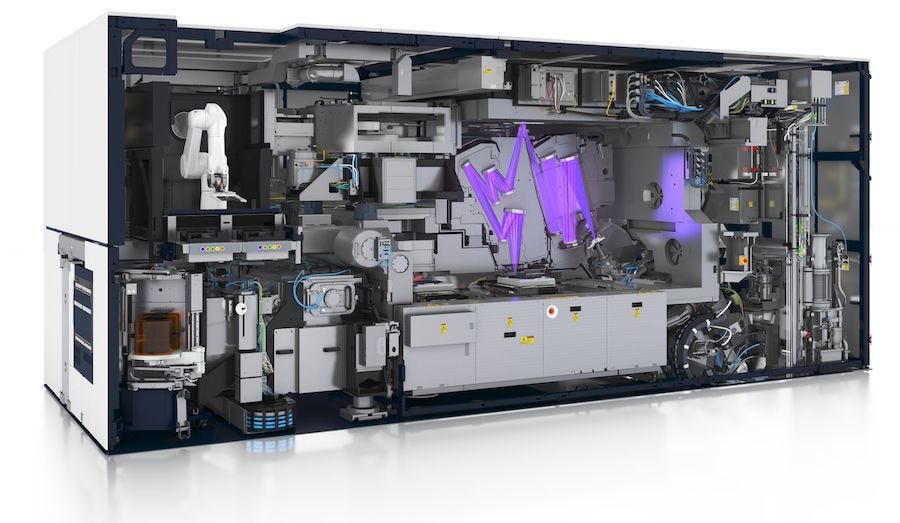
Let’s take a look at the actual production EUV lithography machine ASML manufactures.

As the caption above notes, the full EUV machine is enormous, filling a full room. It is ironic that while computers today are no longer the size of large rooms, the EUV machines that make modern chips required by computers are still enormous! Next, let’s take a look at the core EUV light generation process within the machine.

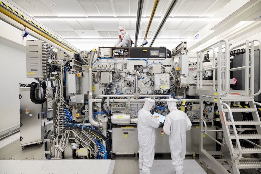
Note the multiple mirrors and the flow of light from the original EUV source up to the mask and the final silicon substrate down at bottom. This entire system has to be maintained within a vacuum because EUV light is readily absorbed by matter. Let’s now look at the actual physical machine with some humans for scale.

Looks very space age! It’s striking just how complicated the entire set up is. Last but definitely not least, EUV machines require sophisticated lasers that can emit focused beams on tight time intervals. Here is a picture of the actual lasers involved.

Discussion
I hope by now you’ve gotten a strong sense of some of the complexities of a modern EUV machine! The economic history behind how ASML was able to design these machines is itself quite complex. ASML was jointly funded by a coalition of TSMC, Intel, and Samsung to the tune of billions of dollars.
The sheer complexity of these machines means that it’s no small task for another company to introduce a competing product to ASML’s. I think therein lies a grand problem for the research community:
How can we build simpler, cheaper EUV machines?
Unfortunately, no research program has yet emerged to simplify these machines and make them easier to build, but I suspect that some targeted funding from US governmental agencies could make a big difference here. Geopolitics in particular requires ASML machines to be tightly export controlled. China is keen to gain access to ASML machines (source) for its domestic foundry efforts.
ASML is a Dutch company headquartered in the Netherlands. While the Netherlands is a democratic country and a close ally of the United states, the Trump years have driven a wedge between the US and the EU. I’m hopeful that the Biden administration can help improve ties between the US and EU, but the EU has also chosen to forge ahead on a closer trade deal with China (source) without involving the US. In a dystopian future, China could one day be able to wield leverage over ASML to prevent shipment of EUV lithography machines to the US!
A theme I’ll return to repeatedly throughout these posts is that technological independence is becoming as important as energy independence. The US should be able to manufacture its own EUV lithography machines or else risk being forced into a weak position one day if access to these critical devices is cut off. I hope researchers and entrepreneurs will take up the challenge of enabling US manufacture of EUV lithography machines!
Next week, we’ll do a deep dive into the physics of EUV lithography.
Highlights for the Week
Deepchem 2.4.0 is out! (source). The DeepChem team has completely rewritten the core DeepChem library to make a modern suite that has PyTorch support, and improved materials science and structural drug discovery tooling along with many ergonomic improvements! DeepChem’s developer team is now international, with students and developers spread across the world (Full disclosure: I’m the lead developer of DeepChem)
Feedback and Comments
Please feel email me directly (bharath@deepforestsci.com) with your feedback and comments! In particular, if you’re currently working in the semiconductor industry, please get in touch! I’d love your input for future iterations in our semiconductor series.
About
Deep Into the Forest is a newsletter by Deep Forest Sciences, Inc. We’re a deep tech R&D company specializing in the use of AI for deep tech development. We do technical consulting and joint development partnerships with deep tech firms. Get in touch with us at partnerships@deepforestsci.com! We’re always welcome to new ideas!
Credits
Author: Bharath Ramsundar, Ph.D.
Editor: Sandya Subramanian
Acknowledgements: Tom Heaps-Nelson, Ph.D.


