The Physics of EUV Lithography
Estimated Reading Time: 10 minutes
Happy Friday! Last week we learned about ASML and its dominant position in the semiconductor industry. ASML is the world’s only supplier of EUV lithography machines and commands a market cap of $220B. We hinted at the difficult physics of EUV lithography in last week’s newsletter, but today we’ll explain more about the actual engineering challenges.
Diving deeper into the physics and engineering of EUV lithography will help us to understand why these machines are so expensive. Along the way we will also see some interesting companies and startups that are working on challenges in EUV lithography. By the end of the post you might have some ideas of your own on how to make EUV lithography cheaper and more accessible!
A Conceptual Schematic
Let’s start with a conceptual overview of the EUV lithography process. At its core, EUV lithography begins with the generation of light at 13.5 nanometers. This light is focused by multiple mirrors, bounced off an EUV photomask to add the stencil pattern (of the chip to be manufactured), and finally focused onto the actual silicon substrate. The diagram below summarizes the process.
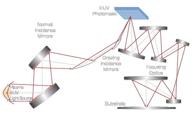
We will review some of the physics of each stage of this process for the remainder of this post.
Generating EUV Light
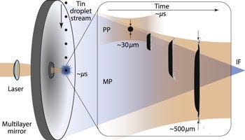
One of the biggest challenges for an EUV machine is the generation of light at 13.5 nm wavelength. The best current method is to create plasma by superheating a gas or metal, usually tin. This excited plasma emits light at 13.5 nanometers which can be subsequently focused using mirrors. The diagram below illustrates the plasma excitation.
This plasma excitation system is quite hard to control. EUV lithography machines today have sophisticated systems to emit precisely timed droplets of tin, which are then hit with a powerful laser beam, superheating the tin into plasma. The heated plasma then emits EUV light, but dissipates considerable energy in the process. Any machine that deals with superheated metal will have serious issues with splatter. Part of the reason that EUV machines are so difficult to deal with is that the tin splatter builds up over time and eventually degrades machine performance, requiring expensive maintenance.
13.5 nanometer light is absorbed by nearly all matter, so this entire system must be maintained in a vacuum, which adds to the complexity of constructing an EUV machine.
Mirrors for EUV Light
One EUV light has been generated, it must be focused and directed to the EUV photomask and then to the silicon itself. It turns out a special type of mirror is needed to reflect EUV light, the Bragg reflector, which is made up of many alternating layers of molybdenum and silicon. See the diagram of a Bragg reflector below.
The Bragg reflectors used in EUV machines are quite complex, with up to 50 alternating layers of molybdenum and silicon. The materials science of creating these mirrors is sophisticated, since each molybdenum/silicon layer must be very thin. The full mirror is a lossy reflector which typically achieves only 70% reflectivity. As depicted in the EUV schematic diagram earlier, the EUV machine requires a series of mirrors (usually 6-12) to focus and direct its EUV light. Combined with the original lossy plasma excitation process, energy loss is a serious concern. In fact, only 1-5% of the input energy reaches the silicon. Reference

EUV Photomasks
The focused EUV light is directed next to the EUV photomask, which overlays a “stencil” pattern of the chip design onto the EUV beam. Conceptually, the stencilling works as illustrated in the diagram below, where the stencil blocks a portion of the source light to create a light pattern of the chip’s desired circuit.

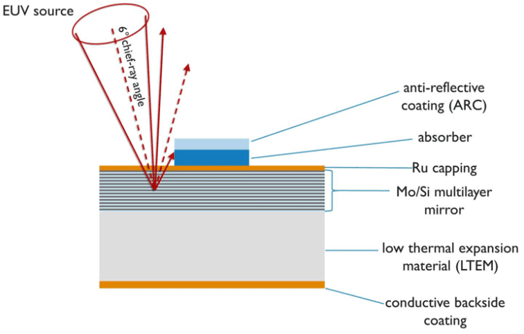
In reality, EUV photomasks are not simple stencils; they are mirrors since the 13.5 nanometer light would rapidly degrade a stencil. Below is a more accurate diagram of an actual EUV photomask. Notice that at the top of the mask is an “absorber”. EUV light is reflected from the Bragg reflector mirror and partially blocked by the absorber. If the absorber pattern absorbs the complement of the integrated circuit, the reflected light will pattern the integrated circuit on the silicon.
There are only a few suppliers of EUV photomask blanks (upon which the absorber pattern for a specific integrated chip can be added) in the world. Asahi Glass Co (AGC) , Hoya, and Applied Materials make these blanks. An EUV photomask blank can cost up to $100,000. Source.
EUV Photoresists
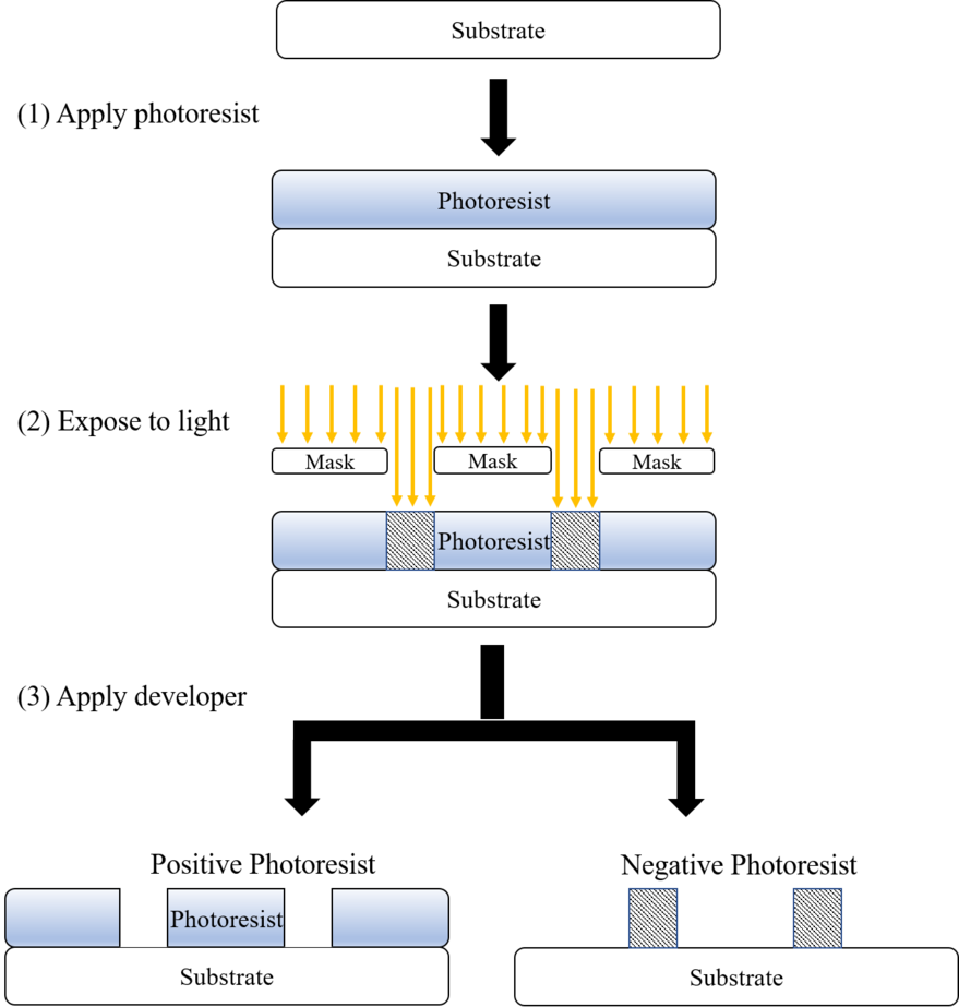
After it bounces off the EUV photomask, the light patterns the integrated circuit design. After reflecting off a few more mirrors, the light hits the silicon substrate. The substrate is covered with a photoresist, which is a special substance that is sensitive to light and that can be easily degraded by light exposure. Without the photoresist, EUV light would have little effect on the raw silicon. The beam of EUV light etches the pattern into the photoresist as shown in the diagram below.
Note that this diagram represents the mask as a physical stencil blocking the light and not reflecting it (the diagram is for an older lithography process, but the conceptual idea is the same for EUV). Heavy energy dissipation (from mirror reflection and from the original tin excitation) causes the EUV beam to have very low power by the time it reaches the photoresist. EUV lithography required the design of special photoresists that were more light-sensitive (Source). One startup to watch in this space is Inpria which recently raised a large series C round.
Noise and Yield Issues
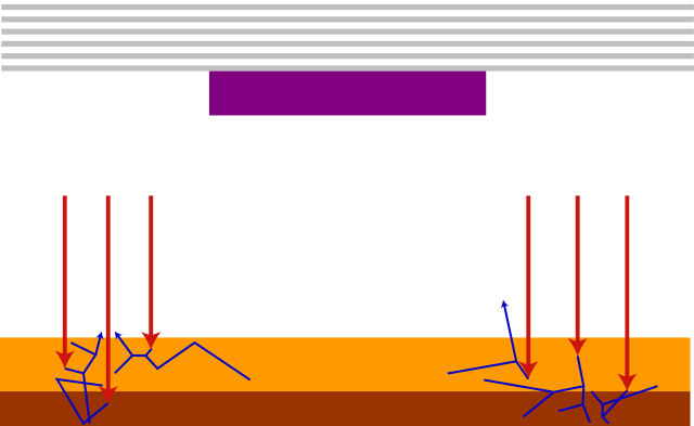
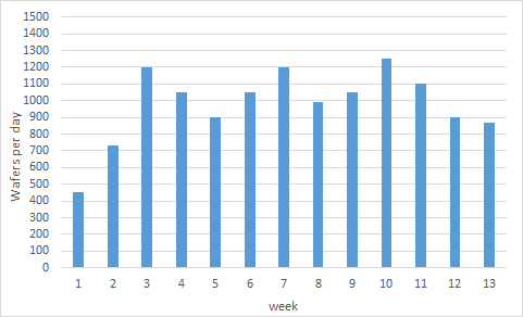
The light/photoresist interaction process is inexact due to the random dissipation of electrons through the photoresist material (see the diagram below). This randomness is a source of concern for EUV lithography, since the chips being created have very small feature sizes (at the 5 nanometer process node). There is a heavy variability in the yield of EUV machines; a number of sophisticated methods (beyond the scope of this post) have been created to deal with noise issues, but despite all the tricks and hacks, EUV lithography remains a difficult process. The second diagram below shows the highly variable yields from one EUV machine. Ensuring robust industrial yields for EUV machines took years of applied research on ASML’s part.
So far we’ve actually only scratched the surface of the complexities inherent in EUV lithography. The wikipedia article has an excellent write-up that I recommend checking out to learn more.
Discussion
Congrats on making it through all the physics! With our improved physical understanding, let’s return to our question from last week:
How can we build simpler, cheaper EUV machines?
Power dissipation is a major issue. Swapping the tin-plasma light generation for a more efficient light source ought to pay dividends, and there are groups working on high harmonic generation lasers which show promising ability to generate EUV light more simply and efficiently. Better distributed Bragg reflectors with lower energy dissipation could also raise efficiency. Finding a way to focus the light without multiple mirrors could also raise efficiency, and better photoresists could lower noise effects and raise machine yields.
To be clear, researchers are working on these ideas already. But there’s lots of scope for improvement. I hope a reader of this newsletter is inspired to come up with an idea of their own!
Highlights for the Week
There’s a lot of Chinese aggression this week.
https://www.ndtv.com/world-news/chinese-fighter-jets-enter-taiwan-airspace-again-2357641: China is flexing its muscles by sending its fighter jets into Taiwanese airspace.
https://www.washingtonpost.com/world/asia_pacific/india-china-clash-sikkim/2021/01/25/7d82883c-5edb-11eb-a177-7765f29a9524_story.html: Chinese and Indian soldiers had a minor clash in the mountains.
Feedback and Comments
Please feel email me directly (bharath@deepforestsci.com) with your feedback and comments! In particular, if you’re currently working in the semiconductor industry, please get in touch! I’d love your input for future iterations in our semiconductor series.
About
Deep Into the Forest is a newsletter by Deep Forest Sciences, Inc. We’re a deep tech R&D company specializing in the use of AI for deep tech development. We do technical consulting and joint development partnerships with deep tech firms. Get in touch with us at partnerships@deepforestsci.com! We’re always welcome to new ideas!
Credits
Author: Bharath Ramsundar, Ph.D.
Editor: Sandya Subramanian
Acknowledgements: Thanks to Tapa Ghosh and Akash Srivastava for a pointer to Inpria on the Twitter discussion of last week’s issue.

