A Crash Course in Transistors
Estimated Reading Time: 7 minutes
TL;DR
In this issue, we will learn some basic transistor physics. We start with an explanation of JFETs (junction-gate field effect transistors) and work up to MOSFETs (metal oxide semiconductor field effect transistors), the most commonly used type of transistor in modern computing devices. We will then learn about modern transistor variants such as FinFETs and GAAFETs, which allow for better miniaturization. Why is it worth learning about the physics of transistors? It’s good general scientific literacy which will let us analyze roadmaps for semiconductor scaling in future issues.
Transistor Basics
Transistors are the foundational circuit elements used in modern computers. The diagram below shows a representation of a modern MOSFET. As a rough explanation of transistor structure, the gate G at the top controls whether current can flow between the source S and the drain D. The transistor provides a switching capability to a circuit to conditionally allow or disallow current to flow. The magic of the transistor is that it transmutes continuous quantities into binary signals: current either flows or doesn’t between source and drain.

Junction-Gate Field Effect Transistors (JFETs)
Before we explain MOSFETs, we will study a close variant, the JFET (junction-gate field effect transistor). A field effect transistor uses an electric field to control whether current can flow through the transistor. By default a JFET is “on”; that is it acts as a conductor between the source and the drain.
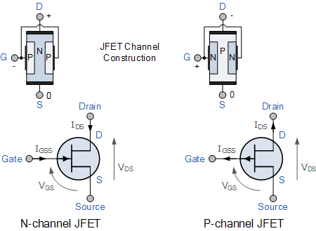
Transistors typically have two types of regions: n-type and p-type. The underlying semiconductor material (usually silicon) is doped by introducing impurities into the crystalline structure (with ion implantation as we saw in a previous issue). If introduced impurities are electron donors, then the doped region is n-type since there will be a surplus of negative electrons. If introduced impurities are electron acceptors, then the region is p-type since there will be a surplus of positive “holes” for electrons. Whenever a n-type region and a p-type region adjoin one another, a depletion layer is created: some of the electrons from the n-type region migrate into the p-type region, depleting the available supply of charge carriers in the n-type region. The diagram below illustrates a JFET with a n-type channel surrounded by p-type gates as well as the induced depletion layers.

Expanding the depletion layer chokes the current flow in the n-type channel. If the voltage between the p-type gate and the n-type source is made negative enough, then the electron donors in the n-type channel will increasingly donate their electrons to the electron acceptors in the p-type gate. As fewer and fewer free electrons are available, the n-type channel is effectively pinched shut. Since the depletion layer switches off the current, we say the JFET is a depletion-type transistor. (Note that the actual behavior of a JFET in the pinched state is more complex than I’ve described here. See here for a more thorough explanation.)

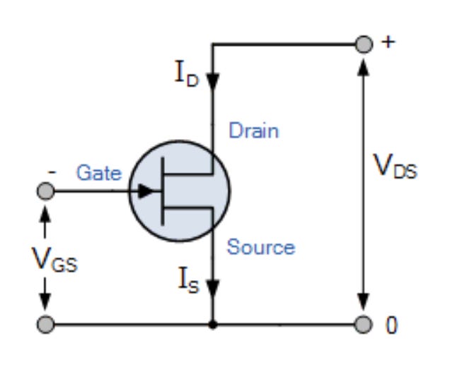
The following circuit diagram schematically illustrates JFET operation. By default the transistor (in the center) is open for current flow, but as the voltage between gate and source drops more negative, the channel will close shut.

So far, we have discussed a JFET with a n-type channel and a p-type gate, but JFETs can alternatively have a p-type channel with a n-type gate. The diagram below illustrates p-type channel and n-type channel transistors side by side. Note how the voltage signs flip for the drain and the gate between the two.

Metal Oxide Semiconductor Field Effect Transistors (MOSFETs)
In a MOSFET, the gate is electrically insulated from the current channel by a thin layer of insulating material. The diagram below illustrates a schematic of a MOSFET. Note the thin layer of insulating material.

Conceptually, a core difference between a MOSFET and a JFET is that MOSFETs can operate as either enhancement type or depletion type. Enhancement type transistors are normally “off”. The application of a voltage to the gate turns them “on” and allows for current flow. Most MOSFETs are enhancement type. The application of an electric field at the gate induces a build-up of charge which can eventually conduct between the source and the drain. In contrast, depletion type transistors are normally “on” and the application of a voltage to the gate turns them “off.” The diagram below illustrates the different types of MOSFETs that can be constructed along with their circuit symbols.

Fin Field Effect Transistors (FinFETs)
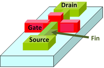
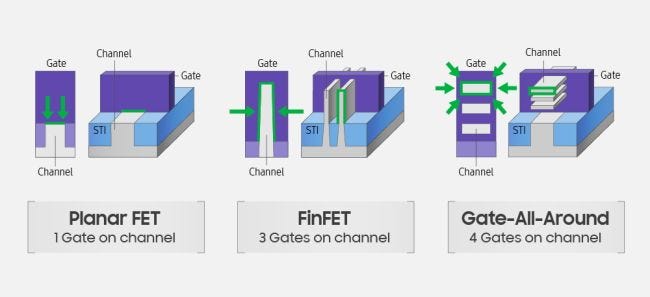
We now have grounding to discuss more recent transistor variants such as FinFETs (see first diagram below). In a FinFET, the gate is wrapped around the channel on multiple sides. The FinFET is a 3D structure as the second diagram below shows. The wraparound gate allows for tighter control of the current passing through the channel. FinFET transistors are used in TSMC’s most recent 5nm and 3nm process nodes (source).


Gate All Around Field Effect Transistors (GAAFETs)
The FinFET wraps the gate around the channel on 3 sides. By simplistic reasoning, perhaps wrapping around the channel on all 4 sides would be even better? Roughly, this is what a GAAFET (Gate all around field effect transistor) does as the diagram below shows. GAAFETs will be used in TSMC’s upcoming 2nm node (source).

Discussion
We’ve done a rapid tour of the different types of transistors commonly used in modern computing devices. Understanding the basics of transistor physics will help us delve deeper into the future of Moore’s law in coming weeks. Next Tuesday, our subscriber-only post will investigate TSMC’s technical roadmap, discussing the changes TSMC sees on the horizon for chip architectures to ensure continuing performance improvements. Subscribe to read along!
Highlights for the Week
https://www.cnbc.com/2021/02/18/biden-to-order-supply-chain-review-to-assess-us-reliance-on-overseas-semiconductors.html: A reassuring step by the Biden administration to review American supply chains.
https://www.timesunion.com/business/article/GlobalFoundries-to-make-military-chips-at-Fab-8-15951541.php: The military is going to start manufacturing chips at a Global Foundries plant in New York. Should reduce dependence on TSMC for critical military needs
https://seekingalpha.com/article/4406598-two-reasons-taiwan-semiconductor-jump-on-intel: A good article discussing why Intel faces serious headwinds competing with TSMC
Subscription, Feedback and Comments
If you liked this post, please consider subscribing! We have weekly subscriber-only posts on Tuesdays.
Please feel email me directly (bharath@deepforestsci.com) with your feedback and comments! In particular, if you’re currently working in the semiconductor industry, please get in touch! I’d love your input for future iterations in our semiconductor series.
About
Deep Into the Forest is a newsletter by Deep Forest Sciences, Inc. We’re a deep tech R&D company specializing in the use of AI for deep tech development. We do technical consulting and joint development partnerships with deep tech firms. Get in touch with us at partnerships@deepforestsci.com! We’re always welcome to new ideas!
Credits
Author: Bharath Ramsundar, Ph.D.
Editor: Sandya Subramanian

