
An Introduction to Semiconductor Foundries
Estimated Reading Time: 7 minutes

Subscribe to our Premium Tier
We’re grateful for all the interest that our newsletter has engendered among the community! “Deep into the Forest” is the first public product from our new firm, Deep Forest Sciences. We plan to produce a high quality free newsletter post every Friday, but are excited to announce that we plan to introduce weekly posts on Tuesdays for subscribers.
Our premium tier newsletter posts will be targeted at deep tech professionals and will analyze company financial documents, investment and entrepreneurial trends, startup formation strategies, and more. We also plan to host interviews with founders, investors, and scientists. Continuing our commitment to highlighting underrepresented voices, we will highlight the work of excellent scientists, investors, and entrepreneurs from these communities.
The premium tier costs $9/month. We hope you will subscribe and help make Deep Forest Sciences a sustainable business that can continue to promote and grow the American deep tech ecosystem!
Semiconductor Foundry Basics
In the last few weeks, we’ve taken a deep dive into EUV lithography and have learned about the economics and physics of lithography. EUV lithography machines are undoubtedly one of the most sophisticated machines used to manufacture modern chips, but modern semiconductor manufacturing involves many more steps.
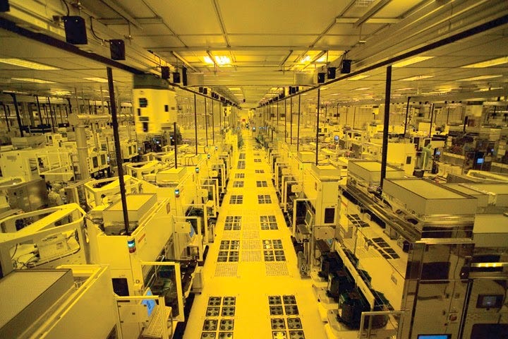
The factories where chips are manufactured are called semiconductor foundries. Building out a full foundry is an immensely expensive task, costing somewhere between $10-$20 billion in investment (source). A modern foundry has many sophisticated instruments in addition to EUV lithography machines. TSMC, the world’s leading foundry company, maintains a series of “gigafabs”, each of which can process over 100K wafers per month (source). Note here that a “fab” is another common term for a semiconductor foundry. Recall that a wafer is a circular disc of polished silicon which is the standard output from a foundry (pictures later in the post). The image directly below is from TSMC’s official site and captures some of the scale and complexity of a modern gigafab. TSMC currently operates 4 gigafabs, which collectively processed more than 8 million wafers in 2019.
As you may now imagine, a modern fab is a sophisticated industrial edifice. This post will be too brief to really explore the complexities of a modern foundry, but will introduce some of the core machines that populate a fab.
Roadmap
The semiconductor manufacturing process starts conceptually from raw sand which is purified into melted silicon. The melted silicon is shaped into high purity silicon ingots, which are then cut into thin wafers. The wafers are polished to mirror smoothness, then carefully cleaned, covered with a protective oxide coating, then with photoresist material, and finally exposed to EUV light from a lithography machine. The photoresist is removed in a development process, and then etching is used to remove portions of the underlying oxide in the pattern of the chip to be manufactured. Ion implantation is then performed to dope exposed regions of the silicon. Modern chips are extremely complex with multiple layers of architecture, so parts of this process are repeated multiple times. Produced chips are carefully tested, since defects can enter at any stage of manufacturing. Even after considerable effort, modern foundries have yields in the range of 30-80% (source). Fabrication of a chip takes on average between 11-13 weeks due to the multiple processing steps and extended testing required (source).
The two diagrams below provide summaries of the semiconductor manufacturing process. The first shows the transformation of raw silicon into a wafer and then into a chip. The second illustrates how the raw surface of the silicon is successively altered by each step in the manufacturing process. In the following sections, we will take a closer look at some of the stages in the manufacturing process.


Growing the Silicon
High quality silicon suitable for semiconductor manufacturing is typically manufactured by the Czochralski process. This process produces single crystal] silicon, which features an unbroken lattice of silicon atoms. High purity silicon is melted in a crucible, and a “seed crystal” is used to guide the formation of the full ingot. Silicon manufactured with the Czochralski process looks visually quite appealing.

The ingot is then sliced into individual silicon wafers about 1mm thick using special diamond-tipped blades (source). These wafers are polished to a mirror smooth surface ready for manufacturing. The image below displays a polished silicon wafer available for purchase from a vendor. The market for high quality wafer producers is competitive and globally distributed (source).

Washing the Silicon
Impurities on the surface of the silicon need to be carefully removed to prevent defects. The standard cleaning procedure, called the RCA process (named for the Radio Corporation of America where this technique was invented in 1965) performs multiple steps of cleaning. The wafers are first washed with a solvent, typically ultrapure water, dipped in a bath of ammonia water and hydrogen peroxide, cleaned with hydrochloric acid, and then rinsed and dried.
Surface Passivation
Surface passivation introduces a thin layer of an oxide over the surface of the semiconductor. At high temperatures, water vapor oxidizes on the surface of the chip to produce a film of silicon dioxide. The picture below shows a furnace used for thermal oxidation.
Photolithography
The previous posts in this series introduced some of the economics and physics of EUV lithography. As a brief recap, photolithography uses light to imprint the integrated circuit pattern onto a chip. There are a number of steps required to prepare the silicon wafer for photolithography. To start, a dehydration bake is performed to completely dry the chip. Next vapor priming (source) coats the wafer with an adhesion promoter such as HMDS to facilitate the subsequent photoresist application (source). The image below shows a vapor priming oven which can apply adhesion promoters to wafers.

Spin coating, in which liquid photoresist is applied to a wafer which is subsequently spun at high speeds up to 10,000 rpm, spreads a thin coat of photoresist over the silicon wafer. The image below shows a photoresist spinner machine. The wafer is soft baked on a hot plate to remove liquid solvent after spinning is complete (source). The processed wafer is then exposed to EUV light in the lithography machine. The image below shows a photoresist spinner.

Etching
Etching is the process of chemically removing layers from the surface of a wafer during manufacturing. The RCA-clean is a type of etching. After the EUV exposure, plasma ashing is used to remove 20-30 nanometers of residue from the top of the wafer to remove any impurities. Multiple rounds of etching are typically applied to the wafer to form required architectural features of the chip in the remainder of the manufacturing process.
Doping / Ion Implantation
The doping process embeds ions into the wafer along regions not covered by the photoresist, which subsequently changes its conductive properties. The diagram below shows how a magnetic field is used to direct ions onto a silicon substrate.

Discussion
This week’s issue toured some of the core machines in a modern semiconductor foundry. In next week’s issue we will continue discussing semiconductor foundries in more depth.
Highlights for the Week
https://www.wsj.com/articles/fords-2021-to-do-list-is-topped-by-fixing-quality-problems-11612450536: Chip shortages are starting to have serious effects on car manufacturing.
Feedback and Comments
Please feel email me directly (bharath@deepforestsci.com) with your feedback and comments! In particular, if you’re currently working in the semiconductor industry, please get in touch! I’d love your input for future iterations in our semiconductor series.
About
Deep Into the Forest is a newsletter by Deep Forest Sciences, Inc. We’re a deep tech R&D company specializing in the use of AI for deep tech development. We do technical consulting and joint development partnerships with deep tech firms. Get in touch with us at partnerships@deepforestsci.com! We’re always welcome to new ideas!
Credits
Author: Bharath Ramsundar, Ph.D.
Editor: Sandya Subramanian