A Deep Dive into Chip Manufacturing: Front End of Line (FEOL) Basics
Estimated Reading Time: 9 minutes
TL;DR
Today’s issue covers chip manufacturing in more depth and introduces its three critical phases: Front End of Line (FEOL), Back End of Line (BEOL), and packaging. The FEOL process builds transistors on the chip, the BEOL process constructs metallic “interconnects” to allow transistors to communicate with one another, and packaging wraps the chip in a supporting case to prevent damage. Each of these steps is very complex, so we start a high level overview of the entire process and then focus on the basics of FEOL processing for today. Next week’s issue will continue the discussion of FEOL manufacturing and following issues will discuss BEOL processes and interconnect challenges in more depth.
Logistics
If you enjoy the writing, please make sure to star the newsletter in your inbox! I’ve heard from some readers that they missed issues since the newsletter was sent to spam or promotions.
A Cross Section of a Chip
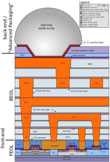
The diagram below provides a schematic of the cross section of a modern chip. At the very bottom, transistors are manufactured by the FEOL process. Directly above are interconnects manufactured in the BEOL process, with multiple layers of copper interconnects spanning different regions of the chip. The packaging layer rests at the top of the diagram and wraps the chip in a protective case. As we saw in this week’s subscriber post, transistor designs will likely grow deeper with additional layers of transistors stacked one atop another, so future cross-sections will only grow more complicated.
An Overview of Chip Construction
As the diagram above shows, modern chips are complex with many layers of interacting components. Modern transistors are also exceedingly small, at the scale of a few nanometers across. At lengths this small, there are only a few tools that modern engineering has for construction. Broadly, these techniques can be divided into additive and subtractive techniques. Additive techniques add a layer of a substance and subtractive techniques remove a layer of a substance. Some examples of additive techniques include deposition and thermal oxidation which can deposit a thin layer of a substance all over the wafer. Note that additive techniques are not typically position sensitive; they tend to spread a thin layer over everything. Subtractive techniques have one powerful advantage compared to additive techniques: they can be easily directed. By using “patterning” techniques such as lithography, specific regions on the wafer can be marked for removal. The most common subtractive technique is etching which can remove a layer of material following a lithographic pattern. Another important subtractive technique is chemical mechanical polishing which can grind off protruding layers on the surface.
Modern chips are constructed in a sequence of additive and subtractive steps which successively build and remove layers on the surface of the wafer. As the cross sectional diagram above shows, chips can have a dozen or more layers, so the construction process can extend to dozens of steps or more. In the next few sections, we introduce some powerful additive and subtractive processes that are used for chip construction.
Chemical Vapor Deposition and Thermal Oxidation
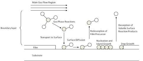
Both chemical vapor deposition and thermal oxidation are used to grow thin films of a material on top of an underlying substrate. These processes can be used to add layers to the wafer in the chip manufacturing process as the diagram below illustrates for chemical vapor deposition.
Chemical Mechanical Polishing
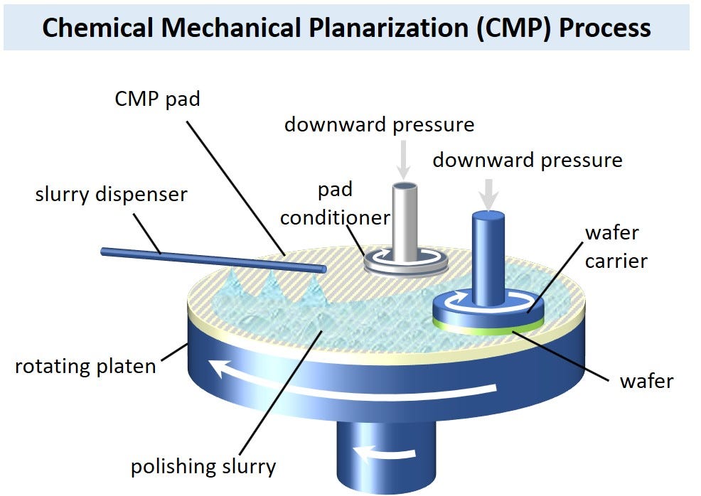
Chemical mechanical polishing (CMP) smooths the surface of the wafer to angstrom level precision. CMP is used at multiple steps of wafer manufacturing to polish the surface of the chip.
Etching and Lithography
Etching is commonly paired with lithography to perform a one-two step of targeted removal. Lithography is used to mark a pattern to be removed and etching is used to perform the actual removal.
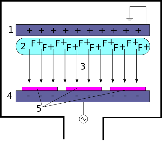
The lithography process starts with application of photoresist, followed by exposure to EUV light from the lithography machine. The photoresist is developed and removed at the pattern marked by the lithography. The exposed oxide is then etched, typically with reactive ion etching which generates ions in a plasma and accelerates them onto the surface. The ions react with the oxide material (coated on the wafer by a previous deposition step) and also remove oxide material directly through kinetic energy transfer. (See the second diagram below.) As an aside, scaling etching to next generation process nodes will require advances such as atomic layer etching.

Shallow Trench Isolation
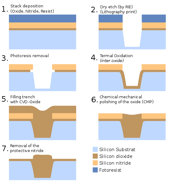
Shallow trench isolation (STI) carves trenches onto the surface of the wafer and fills them with dielectric material to separate transistors and prevent charge leakage. STI is useful as an example of how additive and subtractive processes can be used in sequence to build structures at the nanoscale. The diagram below shows how additive deposition is followed by targeted subtraction (via lithography+etching) and then by more deposition and polishing. Study the diagram and read the caption till you gain a sense for how manufacturing processes work at the chip scale.
Discussion
The construction process for a modern chip requires repeated steps of addition and targeted subtraction. Techniques such as CMP, lithography, etching and deposition are used one after another to build out structures on the surface of the chip at nano-scale. Computer chips are fascinating nano-machines and internalizing their construction process will let us understand other complicated nano-machines that we will review in future issues.
Next week, we will continue the discussion of chip manufacturing by going through the full Front End Of Line (FEOL) process for growing transistors on a wafer. The week after, we will turn to the Back End of Line (BEOL) processes and learn more about how interconnects are constructed. As a sneak peek, interconnects pose major challenges for continued shrinkage of chips, arguably even more so than EUV lithography.
Highlights for the Week
https://www.imec-int.com/en/articles/five-trends-will-shape-future-semiconductor-technology-landscape: A great discussion from IMEC on trends in future semiconductor technology
Subscription, Feedback and Comments
If you liked this post, please consider subscribing! We have weekly subscriber-only posts on Tuesdays.
Please feel email me directly (bharath@deepforestsci.com) with your feedback and comments! In particular, if you’re currently working in the semiconductor industry, please get in touch! I’d love your input for future iterations in our semiconductor series.
About
Deep Into the Forest is a newsletter by Deep Forest Sciences, Inc. We’re a deep tech R&D company specializing in the use of AI for deep tech development. We do technical consulting and joint development partnerships with deep tech firms. Get in touch with us at partnerships@deepforestsci.com! We’re always welcome to new ideas!
Credits
Author: Bharath Ramsundar, Ph.D.
Editor: Sandya Subramanian

