A Deep Dive into TSMC, Part II: The Future of Moore’s Law
Estimated Reading Time: 10 minutes
TL;DR
TSMC has bet on the continuation of Moore’s law as key to its position as the world’s leading edge foundry. At the same time, transistors have reached near atomic scales, calling into question existing strategies for continued transistor miniaturization. Today’s post analyzes TSMC’s research roadmap and explains why TSMC’s Chief Scientist thinks that Moore’s law could last for another 30 years more. In particular, TSMC is betting that continued (but perhaps slowed) improvements in transistor minimization, tighter memory/logic integration, and 3D system integration will combine to extend Moore’s law for decades to come.
Moore’s Law is Still Kicking
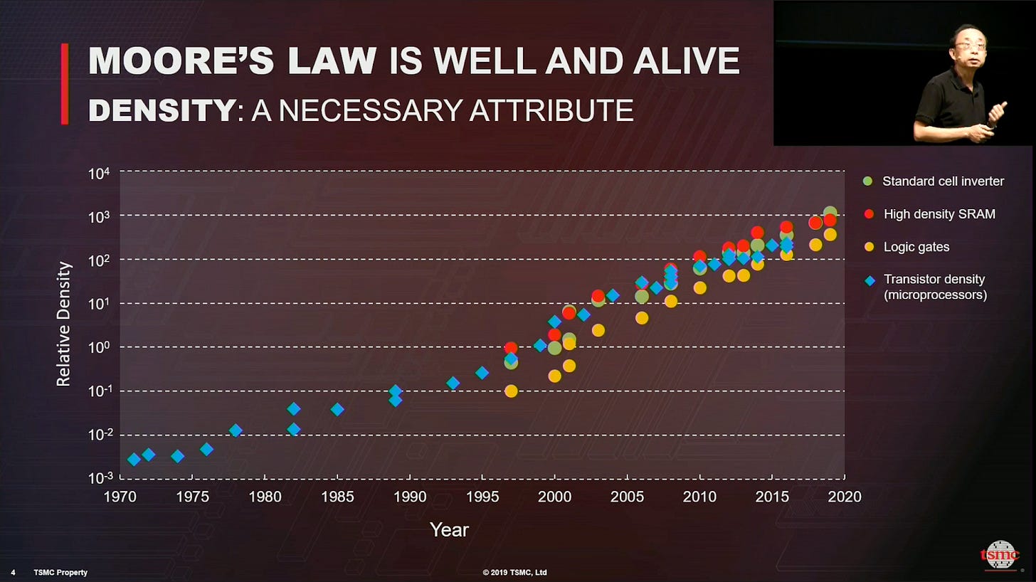
Moore’s law states that the number of transistors in an integrated circuit doubles about every two years. As the following diagram shows, Moore’s law has held over the past 50 years, an extraordinary feat of research and engineering. The slide is from a keynote at HotChips ‘19 given by Philip Wong, a professor at Stanford and Chief Scientist at TSMC. Professor Wong’s talk provides a glimpse into the future as seen by TSMC’s technical leadership

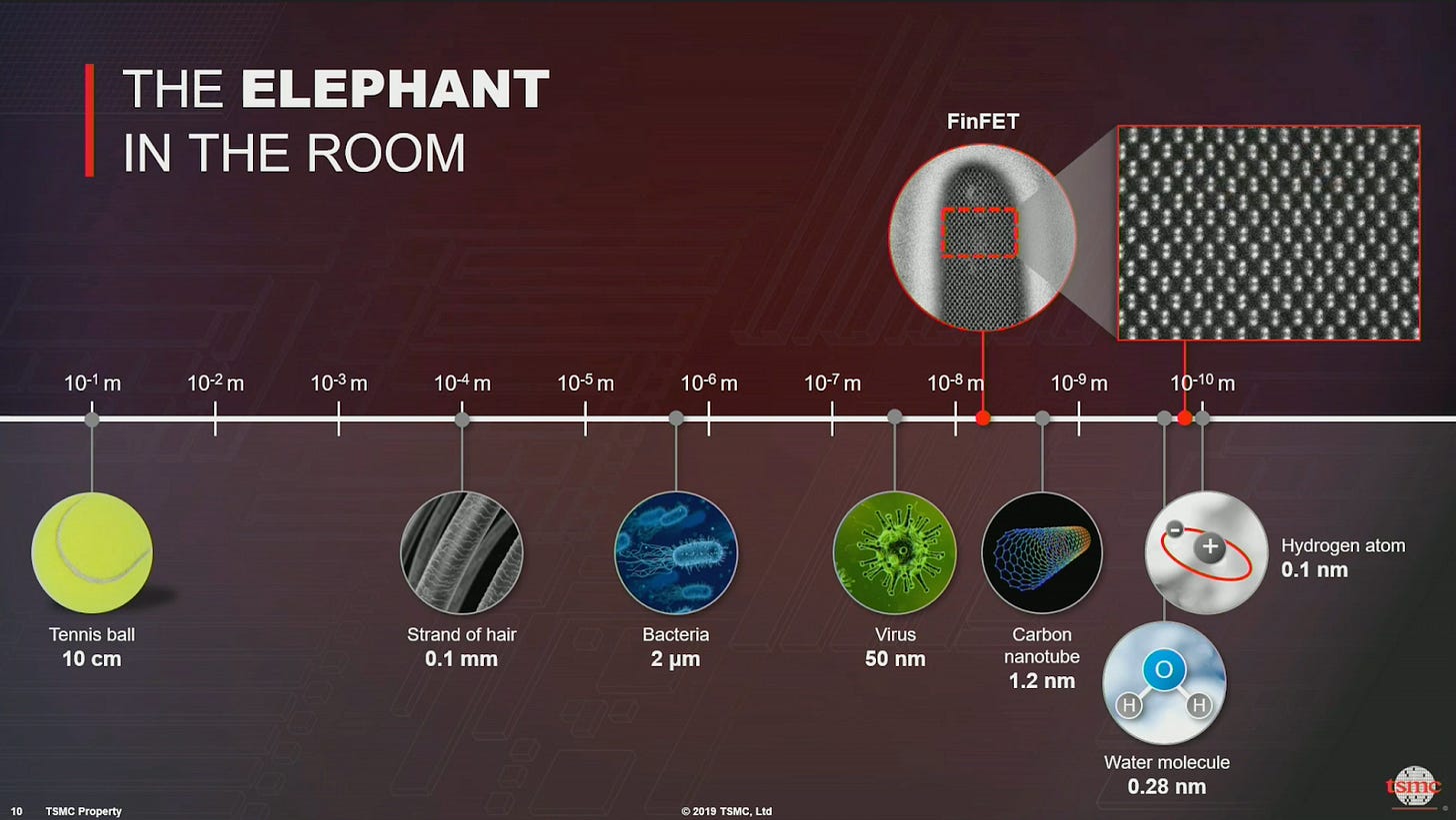
How does the steady and continued improvement on the diagram above match with widespread predictions of the demise of Moore’s law? Part of the challenge, “the elephant in the room” as Professor Wong notes, is that transistors are now so small that scaling will soon hit fundamental atomic size limits. FinFET transistors (see our last issue) are already only a few nanometers wide; carbon nanotube transistors, which are perhaps 5 years from industrial deployment, are a little over a nanometer in size. A hydrogen atom is about an angstrom (a tenth of a nanometer) wide. Single-atom transistors exist but are likely decades from broad use. How can scaling continue given how small transistors are already?

Historically, chips have been planar or nearly planar devices. Stacking transistors in 3D could allow continued densification for multiple generations. As a crude estimate, if each layer were 100 nanometers thick, in principle 10,000 layers could be stacked in a centimeter. Using the fact that 2^13 = 8192, that would give 13 generations of doubling, extending Moore’s law out to nearly three decades! The back of the envelope math of course hides immense complexity, especially since densely stacked transistors would dissipate large amounts of heat.
As an aside, Flatland, a book from 1884 describing a world occupied by two dimensional shapes, was one of my favorite fantasy books in high school. Flatland which poetically describes the complexities of dimension might be good reading for budding chip architects who will need to wrestle with complex 3D designs. Building chips that have 10,000 layers of transistors would be an extraordinary feat requiring major scientific breakthroughs. And yet, Moore’s law has already required 50 years of breakthroughs. Moore himself only expected his observation to extend for 10 years!
TSMC’s strategy is more sophisticated than a simple bet on dimension though. Deep learning workloads are here to stay and have different memory access patterns than classical workloads. Gradient descent constantly refers to and updates large weight arrays in memory. The closer memory can be brought to compute, the faster workloads will run. TSMC has worked to move memory closer to compute with its Chip-on-Wafer-on-Substrate (CoWoS) technology. CoWoS packages multiple dies side by side to allow for high bandwidth interconnects (source). As the slide below from Professor Wong’s talk shows, Nvidia’s latest GPUs use CoWoS to package high bandwidth memory alongside GPU logic to speed up AI workloads.

Summarizing our discussion so far, TSMC’s strategy bets on 3 complementary trends: tighter memory/logic integration, continuing advances in transistor technology, and system integration (roughly going 3D). The slide below summarizes TSMC’s high level strategy as “Multiple Roads Lead to Rome,” where Rome of course is the continuation of Moore’s law. The core difference from classical scaling is that Moore’s law is no longer primarily driven by transistor shrinkage but by multiple parallel engineering trends.

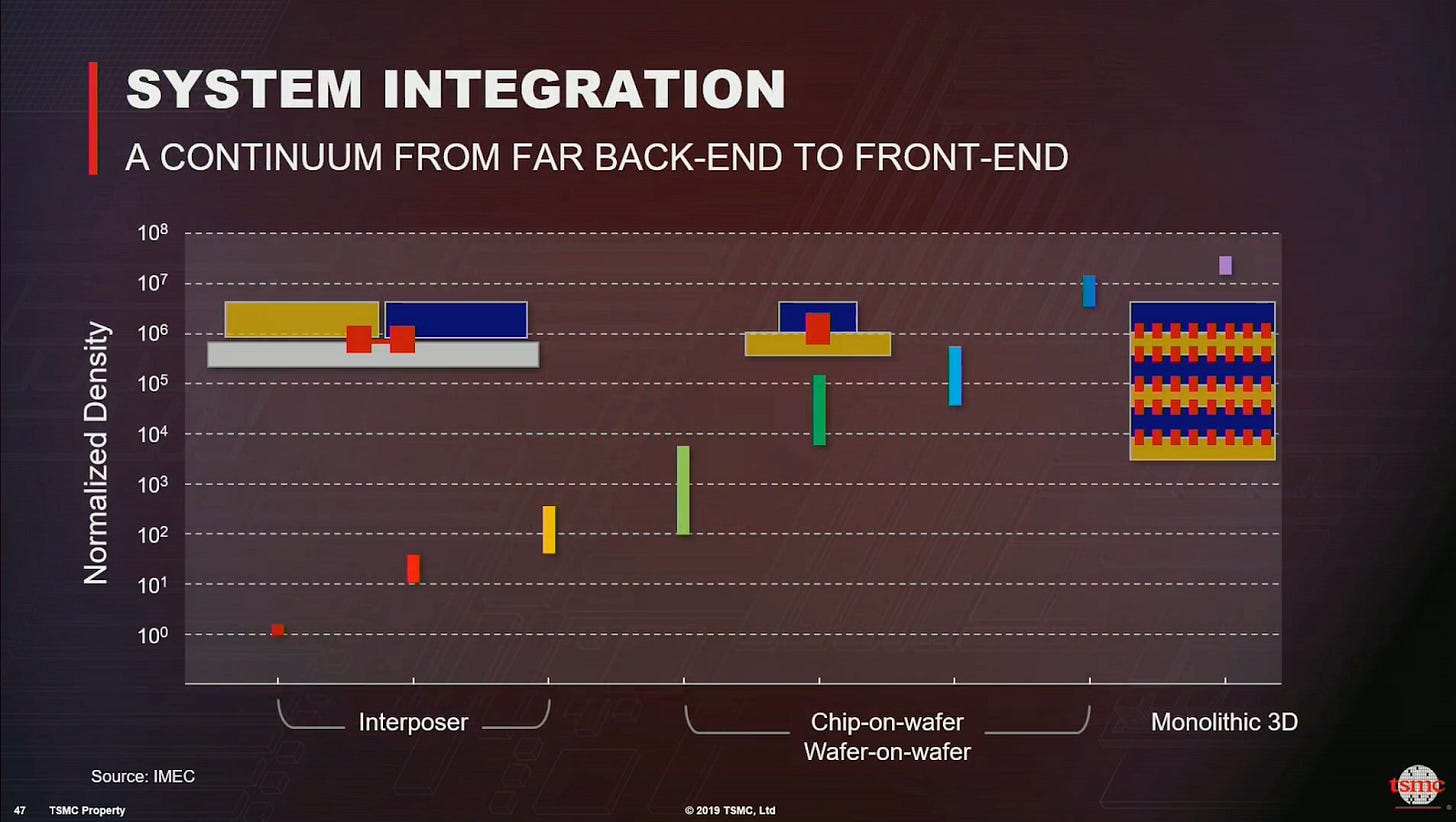
TSMC sees system integration as a core part of its strategy. System integration is a continuation of TSMC’s existing work on CoWoS, but at potentially much tighter scales. As the diagram below shows, moving from CoWoS to 3D integration could yield orders of magnitude scaling improvements.

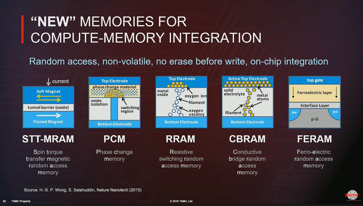
Tighter integration will be driven by advances in nonvolatile memory. RAM is volatile and is flushed when power is turned off. Nonvolatile RAM would blur the boundary between disk and RAM and could permit for fast weight updates in gradient descent. (As an aside, nonvolatile memory could also lead to nightmarish software bugs. Imagine your computer didn’t reset when rebooted! Kernel developers will have to put in hard debugging when these technologies become mainstream.) The slide below shows a few different types of nonvolatile memory that have been developed.

Nonvolatile memory can be integrated directly onto the chip. Systems like CoWoS allow for high bandwidth interconnects between different chips, but directly integrated memory and logic could decrease interconnect latency by orders of magnitude. Professor Wong’s research group has been working on the N3XT architecture for the last several years (see diagram below), which envisions stacking alternating layers of compute logic and nonvolatile memories.

N3XT style chips have been manufactured in academic fabs (source), but with only a few layers of stacking. Deep stacking of compute and logic will require breakthroughs in heat management and rapid manufacturing techniques.
The final layer of TSMC’s strategy is to bet on continuing transistor miniaturization and on two next generation transistor technologies in particular. First, transition metal dichalcogenides (TMDs) are novel types of 2D semiconductors of the form MX2 where M is a transition metal, such as molybdenum, and X is a chalcogen, such as oxygen or sulfur. Transition metal atoms are sandwiched between two layers of chalcogen atoms. The other leading variant is the carbon nanotube transistor. Large advancements in manufacturing will be needed to deploy either of these new technologies at scale. Recent work has made progress moving carbon nanotubes closer to manufacturing readiness. The diagram below illustrates the relative densities of carbon nanotubes, TMDs, and traditional silicon transistors.

Discussion
Let’s return to the important question. Is Moore’s law still alive? Our review of TSMC’s technology roadmap suggests Moore’s law could continue for years to come, but foundational open questions remain. Is it theoretically possible to stack tens or hundreds or thousands of layers in a chip while controlling for power usage and heat dissipation? More accurate simulators could help us answer these questions. Professor Wong’s academic work also uses old lithography technology; better access to cutting edge lithography could enable academics to push research boundaries.
When I started writing, I wasn’t convinced that Moore’s law had legs, but my mind has changed. Major advances are needed, but I can see a future in which Moore’s law continues for decades. Professor Wong didn’t discuss in his talk, but I think that on the scale of decades, Moore’s law will need to leverage advances in quantum computing. Research groups are already working on quantum/classical integration: for example, see recent research from Microsoft on low-temperature CMOS control circuits for superconducting qubits (cite). Perhaps a quantum N3XT multilayer architecture could combine quantum and classical layers on the same chip in a 3D architecture.
Today’s post focuses on the future and is speculative by necessity. Professor Wong’s talk is likely indicative of TSMC’s long term strategy roadmap, but projecting the future of a company decades into the future is a risky proposition at best. TSMC has technical leadership that is committed to maintaining TSMC’s foundry leadership, but the same was true of Intel a decade ago. We will have to see what the future holds!
Feedback and Comments
Thank you for reading our subscriber-only newsletter! We’re still figuring out the rhythm for these posts, so if you have feedback on changes you’d like to see, please send them over to bharath@deepforestsci.com! If you’d like to see more financial analysis, or more technical analysis, or deeper dives into a particular industry let me know and I’ll see what we can do.
About
Deep Into the Forest is a newsletter by Deep Forest Sciences, Inc. We’re a deep tech R&D company specializing in the use of AI for deep tech development. We do technical consulting and joint development partnerships with deep tech firms. Get in touch with us at partnerships@deepforestsci.com! We’re always welcome to new ideas!
Credits
Author: Bharath Ramsundar, Ph.D.
Editor: Sandya Subramanian

