TL;DR
In last week’s issue, we learned about the core machines that populate a semiconductor foundry. In this week’s issue, we will dive deeper into the construction of a foundry and learn about the actual physical edifice itself. Semiconductor foundries are large factories that place considerable burden on the surrounding community and infrastructure. We will learn more about locations that can support a foundry, the noise and architectural considerations needed, and analyze some trends for the future of semiconductor manufacturing.
Foundry Planning
Typically, foundries can only manufacture semiconductors at a particular process node, forcing the construction of new foundries for each new generation of chips. It takes about 2 years to build a new foundry source, meaning that foundry construction has to be planned years in advance of market returns. Foundries for older process nodes are often repurposed to manufacture memory, internet of things or other chips that don’t require cutting edge hardware.
Building a new cutting edge foundry is a major capital investment that requires between $10-$20 billion dollars. World spending in foundries is increasing steadily with about $50 billion total invested in foundries in 2020 (source). The economics of foundries are challenging since large upfront capital is required to construct a foundry that will generate revenue only years down the line. Only the largest companies have the capital access required to fund foundry development (source).
Foundry Location and Environmental Considerations
Potential foundry construction sites cannot have seismic disturbances. The presence of nearby highways, airports, or rail lines can render a site unsuitable for a foundry. At the same time, developers need to be able to transport goods and materials to the site, so potential locations need good road infrastructure.
Foundries also have considerable power and water requirements, requiring robust local utilities that can support manufacturing needs. Taiwan for example is struggling to meet the heavy infrastructural needs of TSMC’s multiple foundries as manufacturing scales up (source).
Clean water requirements for a foundry can be especially challenging. About 2200 gallons of water are required to produce an integrated circuit on a 30cm wafer . A large foundry producing 40,000 wafers per month can use around 5 million gallons of water a day, due in part to the need for ultrapure water for cleaning wafers during manufacturing. Making 1000 gallons of ultrapure water requires 1400-1600 gallons of municipal water. Power requirements for a foundry are also formidable, hitting 30-50 megawatts at peak usage (source). This is about the same amount of power needed by a small city!
Foundry Shell
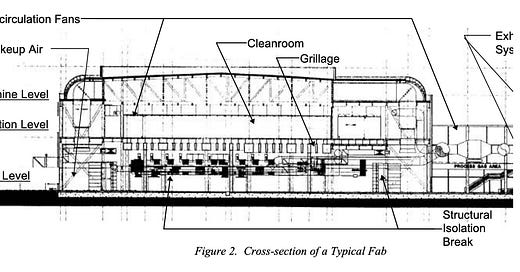
A foundry shell is responsible for protecting the foundry from the surrounding environment. The heart of the foundry is the cleanroom which hosts the machinery that produces new chips. The remainder of the shell is responsible for isolating the cleanroom from the elements to the degree possible. The diagram below provides a cross section diagram of a foundry. Note that considerable structural isolation work is needed to stabilize the production level which contains the cleanroom. The seismic isolation work can end up being the most expensive part of shell construction (source).
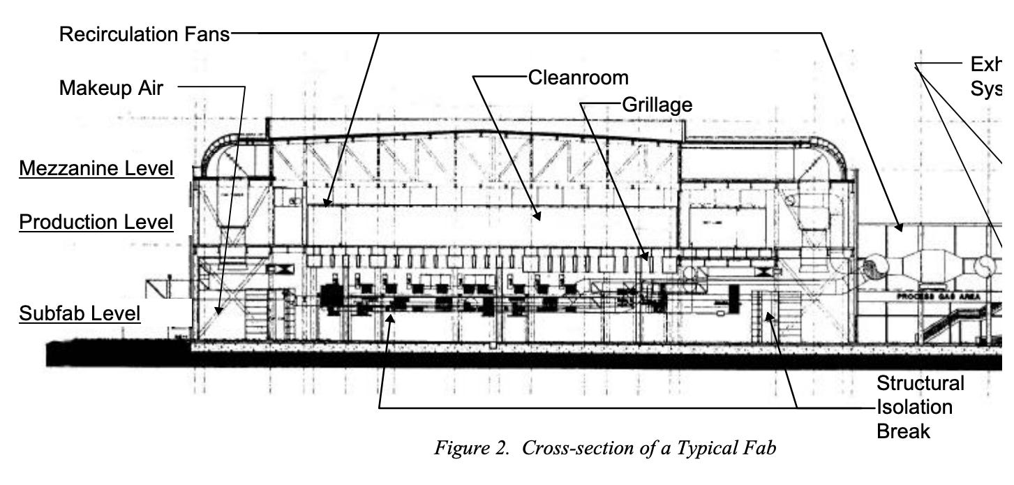
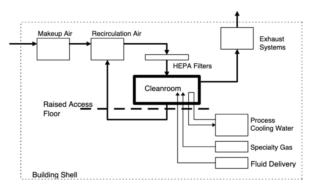
Considerable additional infrastructure is needed to maintain high air circulation. A class 1 cleanroom for a foundry is required to have 600 air changes per hour; a typical office building has about 6 air changes per hour for comparison (source). The “recirculation fans” and “makeup air” system in the diagram above provide a sense of the physical scale of the cleanroom infrastructure needed compared to the cleanroom itself. The diagram below provides a schematic representation of the cleanroom air isolation. Note that HEPA filters are used at the ceiling to filter incoming air and that vents extract air from the floor to recirculate.
One of the major challenges of construction is maintaining clean construction protocols. Dust can get trapped within walls, panels, air ducts and get released into the cleanroom later due to building vibration, which can cause considerable manufacturing defects in produced chips. To avoid these issues, semiconductor companies have to use special construction companies with experience in clean protocols, which require early partitioning of building spaces and repeated cleaning of materials throughout the construction process.
Despite these complexities, construction costs are typically only something like 10-20% of the total cost of the semiconductor foundry. The vast majority of the cost, something between 70-80%, is taken up by the actual equipment inside the foundry. Each square foot of the clean room on average has mechanical equipment that consumes between 100-150 watts of power. Consequently, a foundry with a 100,000 sq. feet cleanroom draws 10,000-20,000 horsepower to power mechanical equipment such as pumps, fans and chillers (source). A lot of the foundry’s equipment is used to further isolate individual manufacturing components. For example, many devices may have individual vibration isolators (see below) to further stabilize equipment.

Selecting the physical layout of devices within the foundry is itself a complex task. Equipment is often placed in an optimized layout to facilitate manufacturing.
Production Ramps
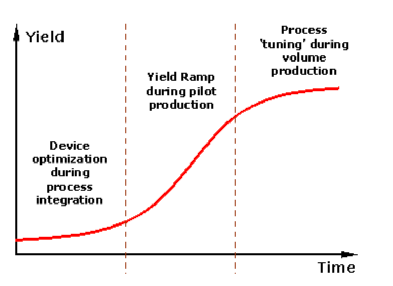
Once manufacturing itself is complete, process engineers will start manufacturing simple chips to verify that all foundry equipment works. SRAM is commonly used to test foundry performance. The name “production ramp” arose since production volumes at a new fab will typically scales up over time as defects and errors in the foundry are fixed (source).
Reducing the Risks of Scale
As we’ve seen in our last few issues, semiconductor manufacturing is immensely complex. The growing complexity has created winner-take-all environments where only the largest companies are able to thrive. The diagram below shows the spread of returns across the semiconductor industry is tightly focused on a few firms.
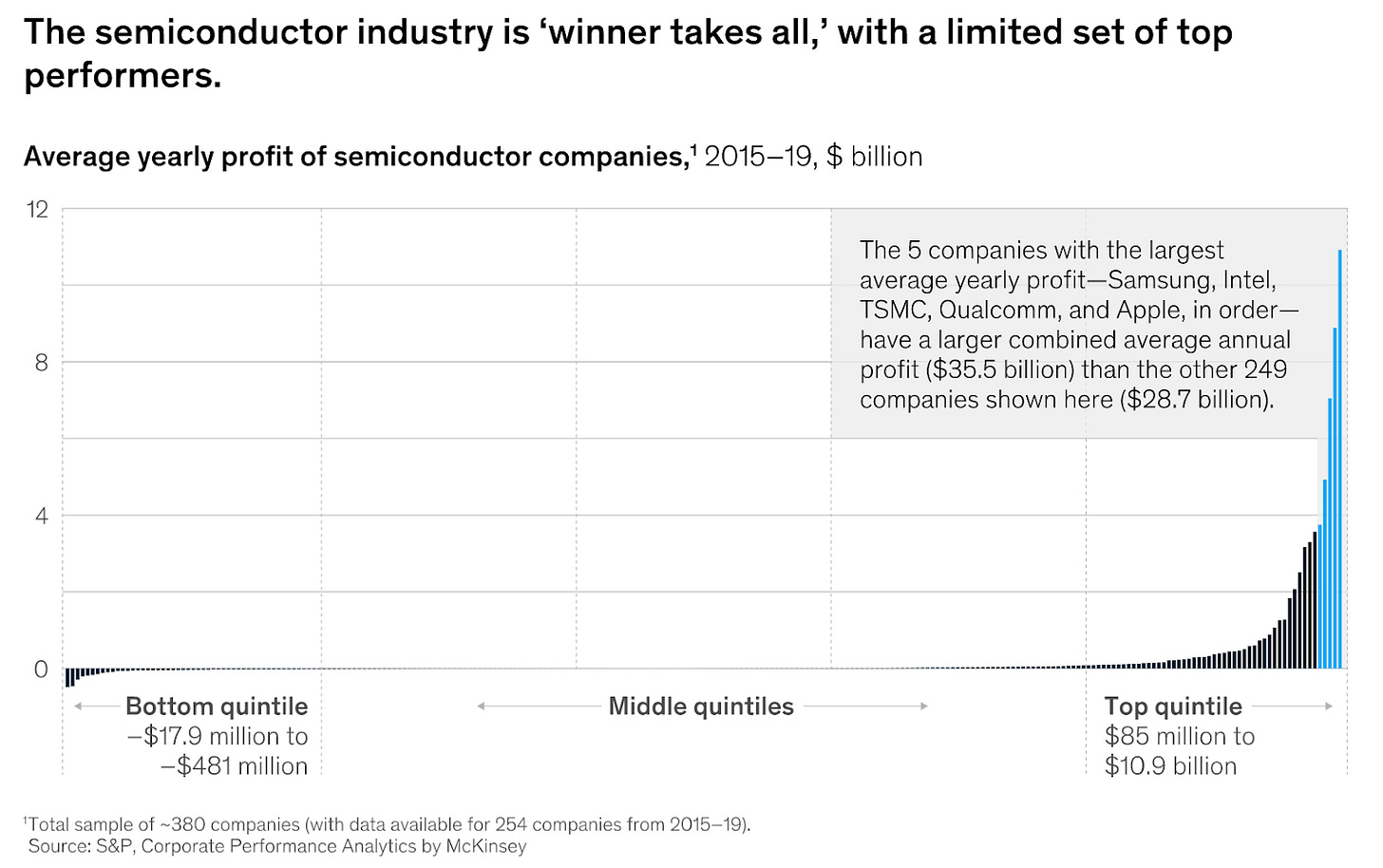
As we have seen in our last few issues, bundling causes risks. Intel’s process failures have driven market share to TSMC and Samsung, both of which operate in China’s aggressive shadow. If you’re Google or Apple, with a trillion dollar market cap, spending $30 billion on a new foundry to ensure the health of your product lines may be a good trade.
I suspect that we’ll start to see the development of experimental in-house foundries within the large tech companies. Apple is rumored to maintain a low volume foundry Athena unit. Apple should consider funding larger foundry experiments to reduce their dependence on TSMC and Samsung.
Returning to the question of risk, governmental agencies can help reduce foundry risk by funding research into affordable semiconductor manufacturing. We need to answer the following question:
How can we build an integrated, affordable and compact semiconductor foundry?
Lights out fabs already have no humans on the manufacturing floor, but I anticipate that we are only at the start of the foundry robotization process. Techniques like deep reinforcement learning could be used to optimize total system yields and to reduce power and water consumption through optimization. Improved physical simulation techniques could improve device efficiencies and speeds, enabling further reduction of cost.
Our next subscriber-only post on Tuesday will do a deep dive into TSMC to learn more about how it has achieved its astounding results over the last few decades. Subscribe to read along! Next Friday, our next free issue will return to basics with an introduction to the physics of modern transistors.
Highlights for the Week
https://asia.nikkei.com/Spotlight/Asia-Insight/Taiwan-s-economy-feels-heat-as-TSMC-feeds-global-chip-boom: A superb discussion of the resource strains Taiwan faces as TSMC ramps up foundry construction.
https://www.anandtech.com/show/16483/samsung-in-the-usa-a-17-billion-usd-fab-by-late-2023: Samsung announcing a large new foundry in the US. A very positive step for US chip independence.
Subscription, Feedback and Comments
If you liked this post, please consider subscribing! We have weekly subscriber-only posts on Tuesdays.
Please feel email me directly (bharath@deepforestsci.com) with your feedback and comments! In particular, if you’re currently working in the semiconductor industry, please get in touch! I’d love your input for future iterations in our semiconductor series.
About
Deep Into the Forest is a newsletter by Deep Forest Sciences, Inc. We’re a deep tech R&D company specializing in the use of AI for deep tech development. We do technical consulting and joint development partnerships with deep tech firms. Get in touch with us at partnerships@deepforestsci.com! We’re always welcome to new ideas!
Credits
Author: Bharath Ramsundar, Ph.D.
Editor: Sandya Subramanian

