How to Build a Transistor
Estimated Reading Time: 8 minutes
TL;DR
Last week's issue covered the additive and subtractive processes that build nanoscale structures on chip wafers. Today’s issue combines these manufacturing steps to explain how to build a transistor. Before technical matters, we will discuss the disturbing trend of rising racism against Asian Americans.
Defeating Racism and Standing Up to China
The last year has seen two parallel and disturbing trends. The first is growing awareness of the horrors of the camps in Xinjiang. Testimonials from the ground allege brutal rapes and other atrocities. Please read these testimonials to understand how serious the situation in Xinjiang has become.
The other trend has been the rise of aggression and racism targeted at the Asian American community. Trump calling Covid-19 the “Chinese virus” has stoked racial fears and prompted disturbing acts. Asian American seniors have been brutally attacked sometimes in broad daylight.
China’s repression in Xinjiang (and Tibet, and Hong Kong) are reminiscent of horrors from colonial times, like Belgium’s atrocities in the Congo, or the United States’ brutality towards Native American nations. The US has not yet reckoned with its past, but we have painfully, fitfully taken some steps toward a more just society, such as with the recent nomination of Deb Haaland to serve as the first native American cabinet member (source). It is not racist to hold China accountable for its horrors, but holding China accountable cannot mean attacking Asian Americans in the US. We must hold up a better alternative to the world against ethnonationalist autocracy by proving that a multi-ethnic democracy can indeed thrive and grow. We all need to stand for Asian American rights.
Here are a few suggestions, sourced from the Antiracism Daily newsletter, on actions you can take. A simple step would be to support your local Chinese restaurant, which may have seen dramatic drop offs in traffic (source). Another would be to support Asian American advocacy groups such as Asian Americans Advancing Justice, AAPI Women Lead, or Stop AAPI Hate. I’ve made a personal donation and I hope you will do the same.
Growing a Transistor Layer by Layer
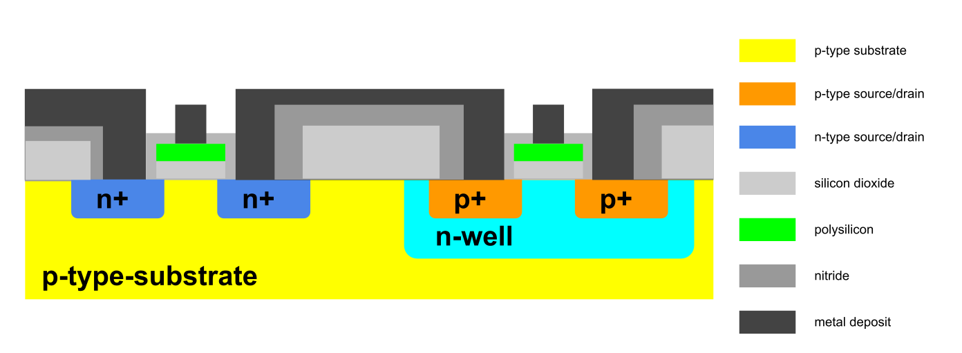
Last week’s issue covered basic nanoscale manufacturing methods. In brief, additive processes add a thin film of material over a surface, and subtractive processes perform targeted removal or smoothing of surfaces. Today’s issue will explain how to build a CMOS inverter at the nanoscale by combining these processes. The CMOS inverter (see diagram below) combines a pMOSFET and nMOSFET and is one of the most widely used circuit elements in modern chips. (See our crash course on transistors for a review of pMOSFET and nMOSFET transistors).

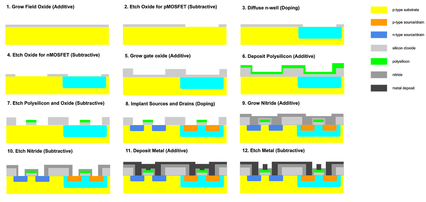
See below for a simplified manufacturing process for the CMOS inverter construction process starting from the raw p-type substrate (recall that p-type substrate is silicon embedded with electron acceptors). When reading through the process, keep the CMOS inverter diagram above in your mind and link each step to a portion of the process diagram above it. Steps are labeled as Additive/Subtractive/Doping. (Doping implants electron donors or acceptors into the raw silicon to modulate semiconductor properties.) Each step builds out one portion of the CMOS inverter using the limited set of additive, subtractive, and doping transformations available.

Grow Field Oxide (Additive): Coat the p-type substrate with protective silicon dioxide. Thermal oxidation is used to grow a layer of silicon dioxide onto the raw p-type substrate.
Etch Oxide for pMOSFET (Subtractive): Use lithography+etching to excavate the pattern for the pMOSFET.
Diffuse n-well (Doping): Embed electron donors at excavated location. Ion implantation embeds electron donors into the substrate, and subsequent annealing diffuses these ions throughout.
Etch Oxide for nMOSFET (Subtractive): Use lithography+etching to excavate the pattern for the nMOSFET.
Grow Gate Oxide (Additive): Grow silicon dioxide to use as the transistor gate. A dielectric layer separates the gate for a MOSFET transistor from underlying layers (see the discussion in our previous issue). Thermal oxidation is again used to grow the gate oxide.
Deposit Polysilicon (Additive): Deposit a thin film of polysilicon over the full system through chemical deposition of silane (SiH4) (source) by the Siemens process.
Etch Polysilicon and Oxide (Subtractive): Use lithography+etching to etch the polysilicon as needed for transistor sources and drains.
Implant Sources and drains (Doping): Implant electron donors and acceptors at the source and drain.
Grow nitride (Additive): Grow a thin film of nitride over the full system as a second dielectric in addition to silicon dioxide.
Etch nitride (Subtractive): Use lithography+etching to excavate the nitride.
Deposit metal (Deposit): Deposit a thin film of metal over the full system. Metal is deposited onto the transistor.
Etch metal (Subtractive): Use lithography+etching to excavate the metal. Notice in the diagram below how metal connections lead upwards out of the gate. These connections will be used in the back end of line (BEOL) process to provide interconnects between different transistors. We will learn more about interconnects next week.
Discussion
The part of the manufacturing process we have covered is typically called the front end of line (FEOL) process as we learned last week. The process we covered is greatly simplified compared to full processes for modern chips which extend to many dozens of steps. Companies like TSMC have built elaborate internal tooling to coordinate these manufacturing steps. Companies that seek to build new foundries must develop their own manufacturing processes that can scale to complex nanoscale constructions.
Next week, we will learn more how interconnects join different transistors on the chip with nanoscale copper wires.
Highlights for the Week
https://spectrum.ieee.org/tech-talk/semiconductors/materials/topological-materials-laser-controlled-new-electronics-medium: Topological materials might allow for the construction of exotic new types of transistors. Swapping to new materials may allow for the continuation of Moore’s law.
https://spectrum.ieee.org/tech-talk/biomedical/diagnostics/quantum-drug: Quantum computing is starting to become robust enough to be useful for drug discovery applications. There are still major scaling challenges here: quantum methods work for 5-10 atom systems, not yet for 30-40 atom small molecule drugs, but quantum computers should scale in the coming years.
Subscription, Feedback and Comments
If you liked this post, please consider subscribing! We have weekly subscriber-only posts on Tuesdays.
Please feel email me directly (bharath@deepforestsci.com) with your feedback and comments! In particular, if you’re currently working in the semiconductor industry, please get in touch! I’d love your input for future iterations in our semiconductor series.
About
Deep Into the Forest is a newsletter by Deep Forest Sciences, Inc. We’re a deep tech R&D company specializing in the use of AI for deep tech development. We do technical consulting and joint development partnerships with deep tech firms. Get in touch with us at partnerships@deepforestsci.com! We’re always welcome to new ideas!
Credits
Author: Bharath Ramsundar, Ph.D.
Editor: Sandya Subramanian


In the first litography+etching step I guess aligning the wafer perfectly isn’t as important. In subsequent litography steps, how do they align the wafer with nanometer precision?