Interconnects: Nanowires on Chips
Estimated Reading Time: 8 minutes
TL;DR
Today’s issue focuses on interconnects, the nanoscale connections between different parts of a chip. These nanowires are responsible for connecting transistors to each other and for wiring power into the chip. We briefly mention the nanoscale manufacturing techniques used to build interconnects and touch on the foundational physics including RC delays. We end by talking about designs for next generation interconnects including new materials and new designs such as the buried power rail.
Basics
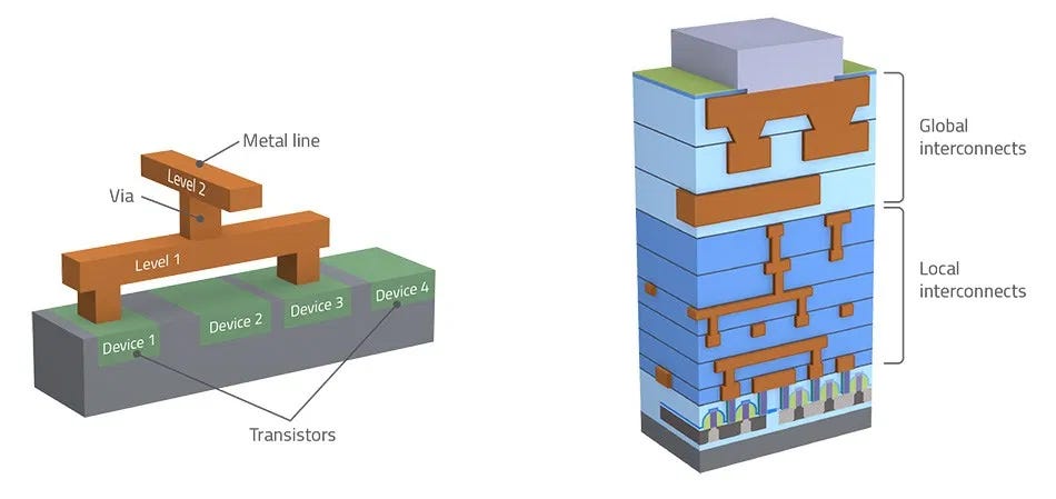
Interconnects connect transistors to one another and provide power into the chip. There are multiple layers of interconnects, typically on top of the raw silicon, that wire different parts of the chip together. The interconnects closest to the transistors are the local interconnects and are very thin to match transistor sizes. Interconnects higher up in the stack are called global interconnects, used to make long range connections and connect to power sources. The layers of interconnects are often labeled M0, M1, etc (for metal layer 0, metal layer 1, etc). Vias are the connections between interconnects at different levels. The diagram below illustrates an interconnect schematic. The entire stack of interconnect infrastructure is usually called the back-end-of-line (BEOL) for the chip. The blue material between interconnects in the diagram below is a dielectric material used to prevent charge buildup.
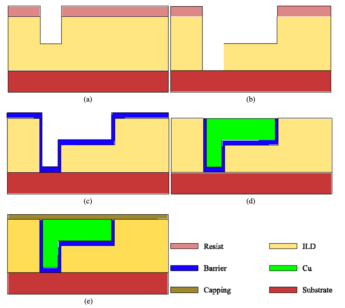
How are interconnects constructed? Deposition is used to deposit layers of dielectric material onto the chip, and then lithography+etching is used to excavate a pattern for the interconnect wires themselves. Deposition is used to fill in the excavated trenches once again with a barrier material and then the interconnect material. Chemical mechanical planarization (see our previous issue) smooths these layers and finally a capping layer is applied. The dual damascene method depicted in the diagram below (the most widespread interconnect technology for copper interconnects) performs a precise series of etching and deposition steps, followed by chemical metal planarization to form the copper interconnect wire structure.
The Basics of Interconnect Physics
A critical interconnect behavior is the RC time constant, where R is the resistance and C is the capacitance. As a review, the resistance of a material is a measure of how easy it is for current to flow through the material. The capacitance measures the charge buildup within the material. As interconnects continue to shrink, both resistance and capacitance have increased, requiring new materials innovation.
A Game of Materials
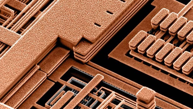
As transistors get smaller and smaller, shrinking interconnects has required the solution of formidable challenges in materials science. Interconnects were originally made of aluminum but swapped to copper due to a breakthrough made by IBM in the mid 90s with the dual damascene method. The diagram below shows an image of a copper interconnect structure on a chip formed using the dual damascene method.
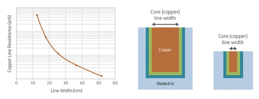
Copper has become unsuitable for transistors at recent process nodes since at smaller scales, copper interconnects cause steep increases in RC delay (see diagram below). As a result, Intel has recently swapped to Cobalt interconnects to lower the RC delay. Newer materials like Ruthenium are being tested for foundry deployment. Even more exotic materials like carbon nanotubes are also being considered for interconnects.
The dielectric layer separating the interconnects has also seen considerable innovation. Another important consideration is that the dielectric constant of the surrounding dielectric should be kept as close to 1 as possible. Manufacturers have turned to “low-kappa” materials which maintain low dielectric constants. Some companies have even turned to introduce air gaps (which have dielectric constant 1) within the chip source.
Middle of Line (MOL) Layer
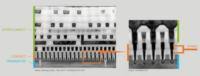
The connection layer between the transistors and the interconnects is called the “Middle of Line” layer and features metal contacts that connect transistors to interconnects. Typically tungsten is used for these contacts, but recently chip makers have started swapping to cobalt which has lower resistance. The picture below shows a cross section of the front-end-of-line (transistors), middle-of-line (contacts), and back-end-of-line (interconnect) layers.
Next Generation Interconnects
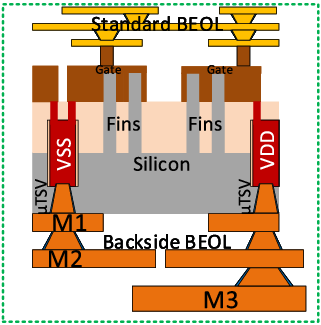
Recent research suggests that moving power rails, which deliver current, directly into the silicon substrate below transistors could drastically reduce complexity at the back-end-of-line layer (source). Buried rails can be made thicker than overhead rails, lowering resistance and preventing voltage drops across the chip. The diagram below from a recent (paper) illustrates a buried power rail system.
Discussion
Interconnects are one of the lesser known parts of a modern chip (as compared with transistors themselves which get more press). However, interconnect technology arguably faces as many challenges as transistor design. Understanding how interconnects work will help build understanding of future generations of processor design. As transistors continue becoming more dense and more 3D, interconnect technology will face formidable challenges, especially with N3XT architectures (see our subscriber issue).
Next Tuesday, our subscriber issue will cover companies that work on tools for electronic design automation. Next Friday, we will discuss packaging techniques which wrap the silicon and layers on top for use in real environments.
Highlights for the Week
https://www.pcworld.com/article/3610750/an-early-review-of-intel-11th-gen-rocket-lake-gives-the-chip-mixed-marks.html: Intel’s latest chip appears to underdeliver on its promises with mixed reviews.
https://mp.weixin.qq.com/s/PlqULXvKfOuEWRy2Isd3gQ?fbclid=IwAR2oEgJDtDttV3xs70sHzm_hIM8dL_pbnDGhYZQty1_itr2GitHQJD5L65k: A review of the Chinese semiconductor ecosystem in Chinese. Link sourced from Jeff Ding’s excellent ChinAI newsletter.
Subscription, Feedback and Comments
If you liked this post, please consider subscribing! We have weekly subscriber-only posts on Tuesdays.
Please feel email me directly (bharath@deepforestsci.com) with your feedback and comments! In particular, if you’re currently working in the semiconductor industry, please get in touch! I’d love your input for future iterations in our semiconductor series.
About
Deep Into the Forest is a newsletter by Deep Forest Sciences, Inc. We’re a deep tech R&D company specializing in the use of AI for deep tech development. We do technical consulting and joint development partnerships with deep tech firms. Get in touch with us at partnerships@deepforestsci.com! We’re always welcome to new ideas!
Credits
Author: Bharath Ramsundar, Ph.D.
Editor: Sandya Subramanian

